The scanning tunneling microscopy and spectroscopy working group is part of the PGI-5, Microstructure Research.

Scientific and technical staff
| Philipp Ebert | Permanent scientific staff (head) |
| Michael Schnedler | Scientific staff |
| Dorothee Rosenzweig | PostDoc |
| Lars Freter | PhD student |
| Yuhan Wang | PhD student |
Recent research topics
Short range ordering in ternary III-V nanowires [1]
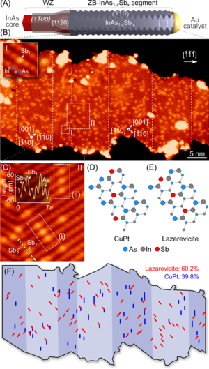
Stabilizing ordering instead of randomness in alloy semiconductor materials is a powerful means to change their physical properties. We used scanning tunneling and transmission electron microscopies to reveal the existence of an unrecognized ordering in ternary III-V materials. The lazarevicite short-range order, found in the shell of InAsSb nanowires, is driven by the strong Sb-Sb repulsion along ⟨110⟩ atomic chains during their incorporation on unreconstructed {110} sidewalls. Its spontaneous formation under group-III-rich conditions of growth offers the prospect to broaden the limited classes of ordered structures occurring in III-V semiconductor alloys.
Quantitative description of photoexcited scanning tunneling spectroscopy and its application to the GaAs(110) surface [2]
We have developed a quantitative description of photoexcited scanning tunneling spectra and applied to photoexcited spectra measured on p-doped nonpolar GaAs(110) surfaces. Under illumination, the experimental spectra exhibit an increase of the tunnel current at negative sample voltages only. In order to analyze the experimental data quantitatively, the potential and charge-carrier distributions of the photoexcited tip-vacuum-semiconductor system are calculated by solving the Poisson as well as the hole and electron continuity equations by a finite-difference algorithm. On this basis, the different contributions to the tunnel current are calculated using an extension of the model of Feenstra and Stroscio to include the light-excited carrier concentrations. The best fit of the calculated tunnel currents to the experimental data is obtained for a tip-induced band bending, which is limited by the partial occupation of the C surface state by light-excited electrons. The tunnel current at negative voltages is then composed of a valence band contribution and a photoinduced tunnel current of excited electrons in the conduction band. The quantitative description of the tunnel current developed here is generally applicable and provides a solid foundation for the quantitative interpretation of photoexcited scanning tunneling spectroscopy.
Importance of quantum correction for the quantitative simulation of photoexcited scanning tunneling spectra of semiconductor surfaces [3]
Photoexcited scanning tunneling spectroscopy is a promising technique for the determination of carrier concentrations, surface photovoltages, and potentials of semiconductors with atomic spatial resolution. However, extraction of the desired quantities requires computation of the electrostatic potential induced by the proximity of the tip and the tunnel current. This calculation is based on an accurate solution of the Poisson as well as the continuity equations for the tip-vacuum-semiconductor system. For this purpose, the carrier current densities are modeled by classical drift and diffusion equations. However, for small tip radii and highly doped materials, the drift and diffusion transport model significantly overestimates a semiconductor's carrier concentration near the surface, making the quantification of physical properties impossible. We apply quantum correction to the drift and diffusion model, in order to account for the so-called quantum compressibility, i.e., reduced compressibility of the carrier gas due to the Pauli principle, in the region of the tip-induced band bending. We compare carrier concentrations, potentials, and tunnel currents derived with and without quantum correction for GaN() and GaAs(110) surfaces to demonstrate its necessity.
Probing defect states in polycrystalline GaN grown on Si(111) by sub-bandgap laser-excited scanning tunneling spectroscopy [4]
Sub-bandgap laser-excited cross-sectional scanning tunneling microscopy and spectroscopy has great potential to investigate the presence of defect states in semiconductors. The characterization method is illustrated on GaN layers grown on Si(111) substrates without intentional buffer layers. According to high-resolution transmission electron microscopy and cathodoluminescence spectroscopy, the GaN layers consist of nanoscale wurtzite and zincblende crystallites with varying crystal orientations and hence contain high defect state densities. In order to discriminate between band-to-band excitation and defect state excitations, we use sub-bandgap laser excitation. We probe a clear increase in the tunnel current at positive sample voltages during sub-bandgap laser illumination for the GaN layer with high defect density, but no effect is found for high quality GaN epitaxial layers. This demonstrates the excitation of free charge carriers at defect states. Thus, sub-bandgap laser-excited scanning tunneling spectroscopy is a powerful complimentary characterization tool for defect states.
Intrinsic electronic properties of high-quality wurtzite InN [5]
Recent reports suggested that InN is a highly unusual III-V semiconductor, whose behavior fundamentally differs from that of others. We therefore analyzed its intrinsic electronic properties on the highest available quality InN layers, demonstrating the absence of electron accumulation at the () cleavage surface and in the bulk. The bulk electron density is governed solely by dopants. Hence, we conclude that InN acts similarly to the other III-V semiconductors and previously reported intriguing effects are related to low crystallinity, surface decomposition, nonstoichiometry, and/or In adlayers.
Strain and compositional fluctuations in AlInN/GaN heterostructures [6]
The strain and compositional fluctuations of nearly lattice-matched AlInN/GaN heterostructures are investigated by cross-sectional scanning tunneling microscopy and selected area electron diffraction measurements in scanning electron transmission microscopy. The presence of strain induces height modulations governed by different roughness components at the cleavage surfaces. The surface height modulations are compatible with a relaxation of alternatingly compressive and tensile strained domains, indicating compositional fluctuations. Changes of the a lattice constant are traced to interface misfit edge dislocations. The dislocations induce steps increasing the roughness within the AlInN layers.
Fermi-level pinning and intrinsic surface states of AlInN() surfaces [7]
The electronic structure of AlInN() surfaces is investigated by cross-sectional scanning tunneling spectroscopy and density functional theory calculations. The surface exhibits empty Al and/or In-derived dangling bond states, which are calculated to be within the fundamental bulk band gap for In compositions smaller than 60%. The energy of the lowest empty In-derived surface state is extracted from the tunnel spectra for lattice-matched AlInN with In compositions of x = 0.19 and x = 0.20 to be E − 1.82 ± 0.41 and E − 1.80 ± 0.56 eV, respectively, in good agreement with the calculated energies. Under growth conditions, the Fermi level is hence pinned (unpinned) for In compositions smaller (larger) than 60%. The analysis of the tunnel spectra suggests an electron affinity of ∼3.5 eV for nonpolar lattice-matched AlInN cleavage surfaces, which is large compared to linearly interpolated values of polar AlN and InN (0001) surfaces.
Polarity-dependent pinning of a surface state [8]
We illustrate a polarity-dependent Fermi level pinning at semiconductor surfaces with chargeable surface states within the fundamental band gap. Scanning tunneling spectroscopy of the GaN() surface shows that the intrinsic surface state within the band gap pins the Fermi energy only at positive voltages, but not at negative ones. This polarity dependence is attributed to arise from limited electron transfer from the conduction band to the surface state due to quantum mechanically prohibited direct transitions. Thus, a chargeable intrinsic surface state in the band gap may not pin the Fermi level or only at one polarity, depending on the band to surface state transition rates.
Omicron VT-STM
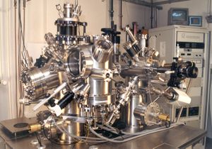
Since the late 90's, our Omicron VT-STM has become the standard working horse instrument for scanning probe microscopy in PGI-5.
- Ultra high vacuum chamber "MULTIPROBE XP" ( mbar)
- System bench with vibration isolation
- Internal eddy current damping system
- Scan range X/Y/Z: 12µm × 12µm × 1.5µm
- Coarse movement X/Y/Z: 10mm × 10mm × 10mm
- Step size: 40nm - 500nm
- Z-resolution: < 0.01nm
- Tunneling current: < 1pA - 300 nA
- Gap voltage: ±5mV to ±10V
- Variable temperature operation in microscope stage (RT - 1500K)
- Low energy electron diffraction
- Auger electron spectroscopy
Software
STM Analyzer
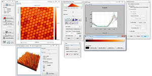
The STM Analyzer is a powerfull means to open and analyze scanning probe microscopy images and spectroscopy data sets. The current version supports the following data formats:
- Omicron SCALA
- Omicron MATRIX
- RHK SM4
- ProDas TU2
- Digital Micrograph DM3
- Ascii/Bmp images
The software is and was developed by our STM group and is written in Object-Pascal (also known as Delphi/Lazarus). A incomplete feature list is given below.
- non-linear slope substraction
- drift correction[9]
- spectroscopy processing, including offset-substraction
- automated evaluation and sorting of spectra (by set-point comparison)
- three dimensional visualization of measured data
- image filters (Gaussian, FFT, color remapping, differentiating)
P_SpaceChargeLight
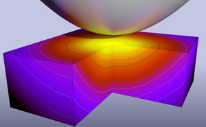
P_SpaceChargeLight is a tunnel current simulation software package that is developed by Michael Schnedler. It accounts for the influence of the electric field of a metallic probe tip in proximity to a semiconducting surface by solving both, Poisson- and continuity equations for holes and electrons within a semiconductor in three dimensions, prior to the derivation of the tunnel current. Due to the solution of the continuity equations, P_SpaceChargeLight is capable of simulating the redistribution of non-equilibrium charge carriers that are created e.g. by band-to-band transitions due to laser irradiation. The numerical Poisson- and continuity equation solver is based upon a finite-difference scheme. Rotational symmetries are not included due to reasons of universality (e.g. non-symmetrically tips). The tunnel currents are computed in Bardeens approximation[10], which was further developed and adapted by Harrison[11], Bono and Good[12], as well as Feenstra[13]. The potential and carrier concentrations along the central axis through the tip-apex is used to derive the tunnel current in a one dimensional approximation. Additionally, excess carriers are included in the tunnel current computation by introducing quasi Fermi levels.
P_SpaceChargeLight was developed "from scratch" and is written in Pascal (software can be compiled for any operating system, since it does not make use of WinAPI).
References
- ↑ https://journals.aps.org/prb/abstract/10.1103/PhysRevB.94.195306
- ↑ https://journals.aps.org/prb/abstract/10.1103/PhysRevB.91.235305
- ↑ http://dx.doi.org/10.1103/PhysRevB.93.195444
- ↑ http://aip.scitation.org/doi/full/10.1063/1.4972563
- ↑ http://dx.doi.org/10.1103/PhysRevB.94.245201
- ↑ http://dx.doi.org/10.1063/1.4963184
- ↑ http://aip.scitation.org/doi/10.1063/1.4973765
- ↑ http://dx.doi.org/10.1103/PhysRevB.91.205309
- ↑ http://dx.doi.org/10.1016/j.ultramic.2013.08.004
- ↑ https://doi.org/10.1103/PhysRevLett.6.57
- ↑ https://doi.org/10.1103/PhysRev.123.85
- ↑ http://dx.doi.org/10.1016/0039-6028(86)90243-8
- ↑ http://dx.doi.org/10.1116/1.583691
