Michael Schnedler
A member of PGI-5 Institute for Microstructure Research.
Research
Being member of Scanning tunneling microscopy and spectroscopy group, my research is dedicated to following projects:
- Characterization of novel (ternary) nitride semiconductors by scanning tunneling microscopy (STM) and spectroscopy (STS), e.g. GaN, InN, AlInN, AlGaN, etc.
- Defects in (light-excited) semiconductors and their influence on the electric properties
- Investigation of device structures like LEDs by STM
- III-V compound semiconductor nanowires for future lighting applications or energy harvesting
Publications
Updated list of publication can be found at ORCID and ResearchGate.
Expertise

- Quantitative STM and STS of III-V compound semiconductors (including nitride-based semiconductors)
- Sample preparation for STM & STS
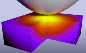
- Simulation of potential & carrier distribution in semiconductors under non-equilibrium conditions
- Tunnel current simulations (including tip-induced band bending)
- Principal component analysis
- Software development (for analysis and simulation) primarily by using Pascal, but also Python, C, PHP, etc.
Contact
Email: m.schnedler@fz-juelich.de
Phone: +49 2461 61 3155
Location: Building 04.6, room 98